Hardware Design Updates

This post concerns the Open ARDF Equipment Project, which is utilizing the Receiver Development Platform, both of which are being developed together.

With the basic components for serial communications and bootloading identified and verified experimentally, it was time to take another look at the schematic. Only the transmitter schematic has been updated, but as far as the USB/FTDI changes are concerned, the same circuitry will go into the receivers as well.

Since changes were being made to the schematic anyway, it seemed like a good time to examine the transmitter’s DC-power control circuitry. Below is a summary of the transmitter schematic changes that were made, and the features those changes support. Schematics have been posted.

DC-POWER CHANGES

Master On/Off Switch – A single SPST switch was added. Turning it off removes all LiPo/Li-Ion battery power going to the transmitter, while still allowing the battery to be charged via USB.

Direct Processor Power – The processor is continuously powered directly from the LiPo/Li-Ion battery as long as master power is turned on. There is no provision for powering off the processor except via master on/off.

Processor Power Control – The processor is given the means to shut down all power to every part of the transmitter, except for the processor itself. Thus the processor is in full control of current drain, and should be able to bring the total current drawn below 1mA by shutting down all devices under its control, and putting itself into a low-power sleep mode.

Processor Wake-Up – Even in a deep-sleep low-current mode, the processor can be awakened by an interrupt received from the real-time clock. The processor can schedule an alarm time (e.g., competition start time) at which to be awakened.

Antenna Disconnect Protection – Provision has been made to automatically shut down all power to the transmitter (except to the processor) in the event that the antenna is disconnected. This will prevent the transmitter from being damaged by operating into an absent antenna, and is also intended to be the primary way to turn on/off the transmitter when it is deployed or collected: just plug in the antenna and you’re all set.

USB-to-UART CHANGES

The following features are supported by the FTDI circuit changes applied in the schematic:

Processor Power from USB – Even if the master power switch is in the off position, connecting the transmitter to a USB power source will power up the processor. This way it will always be possible to bootload, or change transmitter settings, via USB even if the transmitter is powered off.

FT232R Device Optional – The builder can decide whether or not to populate the FT232R USB-to-UART IC. The option to instead use an “FTDI Cable” (like this one) is supported by the inclusion of a 6-pin male header.

USB Compliance – Circuitry has been added to ensure that the transmitter draws no more than the USB standard-specified current and prevents excessive surge current.

LED Data Indicators – Red and green LEDs indicate when data is flowing on the serial data lines.

Cloning – It will be possible to “clone” transmitters by connecting their serial ports using a “null modem” cable. This will allow any transmitter to be designated as “master”, and by connecting it with another “slave” transmitter will synchronize the slave’s clock, and configure the slave to operate of the appropriate frequency and sport mode. This should eliminate the need for a Control Head, or a PC, in many situations once a single transmitter (the master) has been configured.

Hardware UI

This transmitter design incorporates a simple interface for the user: a push button, an LED, and a power switch. Additional feedback to the user can be accomplished via radio, by having the transmitter send pico-power transmissions (with the power amplifier turned off), that can be monitored up to a few meters away using a handheld receiver. The intent is for these to be used for basic configuration settings (such as “fox number” and activity type), and to trigger status feedback from the transmitter.

The serial interface should make it easy to configure any setting, including “call sign”, clock synchronization, automatic start time, and every other function and feature the transmitter provides. A program running on a PC/Mac/Ubuntu will provide a simple and intuitive graphical user interface, or menu-driven format. In a future version, an app running on a smartphone could provide the interface and configure the transmitter conveniently over WiFi. The button and LED is for those times when a computer is impractical or unavailable.


Beware DebugWire When Reset Doesn’t

This is just a note to all, and to remind myself:

Are you having difficulty getting your ATmega to reset properly using the external Reset pin? Do all the other resets (watchdog, brown-out detect, and power up) work just fine, but the processor always locks up immediately after a negative pulse on the Reset pin? Have you been using debugWire to flash the processor or to debug?

This might be the answer you seek: Note that if debugWire is enabled, the external reset will not function properly: so check to make sure you have disabled debugWire before attempting to reset the processor using the Reset pin. Needless hours can be wasted searching for the cause of a malfunctioning Reset pin – I know that for a fact – so don’t overlook this potential cause for the problem.

Here are the pertinent paragraphs from the ATmega data sheet:

25.5  Limitations of debugWIRE

The debugWIRE communication pin (dW) is physically located on the same pin as External Reset (RESET). An External Reset source is therefore not supported when the debugWIRE is enabled.

PC Interface! Bootloader!

This post concerns the Open ARDF Equipment Project, which is utilizing the Receiver Development Platform, both of which are being developed together.

There has been a good deal of progress on the Dual-Band Receiver project this week, mostly on the software front.

This week I received an order from AdaFruit that included an FTDI Serial TTL-232 USB cable. That cable is, essentially, a USB-to-UART converter. Drivers for that cable are available for all the popular computer operating systems: Linux, OS X, Windows. Installation was a snap. I just plugged it into a USB port on and my computer, and it found and installed the appropriate drivers with no issues. My computer then showed a new serial port available: COM3 on Windows.

Only three wires from the FTDI cable needed to be connected to the Digital Interface Board: RX, TX, and ground. After wiring it up, installing a terminal emulator (PuTTY), and setting the baud rate to 9600 baud, the PC was able to “talk” to the Dual-Band Receiver’s Digital Interface Board. This opens a new universe of possibilities for the project.

PC Control

Using the serial interface provided by the FTDI cable, it is now possible to control the Dual-Band Receiver using the same Linkbus messages used for communication between the Digital Interface Board and the Control Head. So, from the PC, one can set the band, frequency, volume, monitor signal strength and battery level, etc. just like one does using a Control Head. The only difference being that you need to type in the correct Linkbus messages and then interpret the response messages from the receiver.

PC control could be made much more convenient by writing a PC application to provide a nice GUI interface for the user. One might have a graphical image of a receiver on the PC display, and by interacting with the image (turning dials, flipping switches, etc.) the PC application would apply those settings to the receiver over the Linkbus FTDI-cable interface. But just having some icons, buttons, or text boxes would make setting the receiver intuitive and effortless, with no need to memorize the Linkbus message protocol.

PC control, even without a GUI receiver application, means that it is no longer necessary to build a Control Head in order to test and experiment with the Dual-Band Receiver. This should make it much easier, and less costly, for anyone wanting to experiment with the receiver. The same capability will be added to the transmitter too.

Bootloader

The serial interface also provides the communication support required for bootloading. A bootloader is a small software program that resides in a special memory location in the microcontroller: a segment separate from the main program memory. The bootloader gets called immediately after the ATmega328P resets (or powers up), and before control is passed to the main program. The bootloader automatically checks the processor’s UART to see if a PC (running a special programming tool) is connected, and if one is present the bootloader supports writing new software into the ATmega328P, updating the main program.

A bootloader simplifies the process for updating the receiver software because updating can be done without the need for an “In-System Programmer” (ISP) device. Instead, all you need is the FTDI cable. Better yet, once the FTDI chip is added to the receiver design, you will only need a standard USB cable, such as the one that comes with most commercial electronic devices (cell phones, cameras, etc.) that connect to computers. We should also be able to utilize the DTR signal line coming out of the FTDI FT232RL chip, allowing the programmer to automatically trigger a reset just prior to programming the device.

Open source bootloader software is available on GitHub. Using the Optiboot source code, it was possible to create an Atmel Studio project that builds, installs, and debugs a simple bootloader for the Receiver Development Platform. A simple bootloader is working as of now, and has been used to successfully update the software on a Digital Interface board. This was accomplished running AVRDude on the PC: the same free software updater program many Arduino experimenters use.

Since we can now build and modify our own bootloader, we have total freedom in making it work the way we want. So we should be able to make it work conveniently for the user. Perhaps even making it possible for a future version of the Control Head to apply software updates to an attached receiver or transmitter.


Software is on GitHub

There is still plenty of work to be done on the software, but it is functional as a basic dual-band receiver, and potentially useful for others. So I’ve cleaned it up, added the MIT License language as a header to each file, and posted it all on GitHub: https://github.com/DigitalConfections/Receiver-Development-Platform

I will continue to update the software as regularly as I can, especially since I will be using git (and the GitHub repository) for configuration management and archiving.

Licensing is the least restrictive that I could find. You can pretty much do anything you want to with it. Enjoy! But if you identify ways to improve it, I would much appreciate it if you would submit your improvements to the project.

Receiver Progress

This post concerns the Open ARDF Equipment Project, which is utilizing the Receiver Development Platform, both of which are being developed together.

The linear power regulators have been installed and tested on the Receiver board, along with the PCF8574A I2C port expander IC. A simple driver for the port expander was written and shown to work to control and read the port expander pins. The SA605 receiver IC was installed, along with the filters and supporting components. The Digital Interface board was then plugged into the Receiver, and the entire system of three boards was powered up and tested.

The receiver now operates on 2 meters: the Control Head allows the receiver’s operating frequency to be set, and the received signal strength is shown on the display. The receiver itself is lacking in sensitivity, but it does receive strong signals injected into the matching circuit connected to the SA605 input.

Lacking an oscilloscope, the following test set-up will be used to investigate and tweak the receiver sensitivity:

Receiver Test Set-up Diagram

Click on the above image for a closer look. The original Receiver Development Platform experimental boards (built several months ago) will be used as a precision VHF signal generator. An adjustable 100dB attenuator will allow precise control over the signal level delivered to the receiver under test by the signal generator. Instead of probing test points using an oscilloscope, a VHF all-mode receiver will be used; its RF input attenuated by a second adjustable attenuator. It is hoped that this will allow very low signal levels to be generated, and probed at board level. The receiver’s S-meter will provide a rough estimate of the absolute signal levels, while the precision attenuators should provide a way to obtain reasonably-accurate measurements of changes in signal strength.


Display Interface Taking Shape

This post concerns the Open ARDF Equipment Project, which is utilizing the Receiver Development Platform, both of which are being developed together.

A rudimentary linkbus is now in place, allowing the Control Head and the Digital Interface to exchange information with one another. The two recognize when the other device is sharing the bus, and behave accordingly. When connected to a Digital Interface, the Control Head displays a special dual-band receiver screen that shows a (growing) number of receiver settings and related information. Below is a picture of the receiver display as it stands right now:

Receiver Display for 145.52 MHz

The four white dots across the top of the above image are the menu buttons. Immediately below the buttons, printed across the top row of the LCD, are labels indicating the current function assigned to each button: Button 1 sets the band (it is currently set to 2 Meters), Button 2 sets the active memory location (currently memory Location #1), Button 3 sets the received signal parameter (currently Radio Signal Strength), and Button 4 sets the auxiliary function (currently Time of Day). Below the button labels is receiver information: the receiver is currently set to 145.5200 MHz, the received signal strength is 9, and the time is not yet implemented (blank).

Just below the display is the knob of the rotary encoder. Depressing the rotary encoder knob activates another switch. A long press (>3 seconds) on the knob enters the Frequency Edit mode, and a blinking cursor appears (see below) indicating the digit to be incremented (or decremented) by turning the dial. Tapping the knob advances to the next digit; turning the knob changes the value of the digit. Frequency Edit mode is exited by another long press on the knob, or simply by taking no action for 5 seconds.

Editing a 2m Frequency

The * next to the MEM4 label in the image above indicates that the frequency has been changed, and now differs from what is stored in memory Location 4. The frequency setting can be saved to MEM4 by pressing and holding the MEM4 key for about 3 seconds. Changing to a different memory location (by tapping the MEM4 button) will lose any changes made to the frequency setting. Each band has its own set of five memory locations.

The image below shows an 80m memory location being edited, with the kHz digit being changed.

Editing an 80m Frequency

Although a signal strength is indicated, there is no analog radio circuitry built yet. The correct VFO and BFO signals are being set in the Si5351, and the audio gain level can be adjusted, but the receiver itself is still absent. The RSSI is just noise at the ATmega328 ADC input, but it is a real value being measured and reported by the Digital Interface and being sent to the Control Head over the linkbus. This should make for a convenient test platform for the Receiver board, which will get populated next. And once the Receiver board is working we will have a functional, if simple, ARDF receiver.

Control Head In a Box

There has been a good deal of progress on both the hardware and software fronts. Button “plungers” of the proper length arrived, along with nuts and bolts (2mm size) to retain the display in the transparent lid, so it is now possible to see how a Control Head will look:

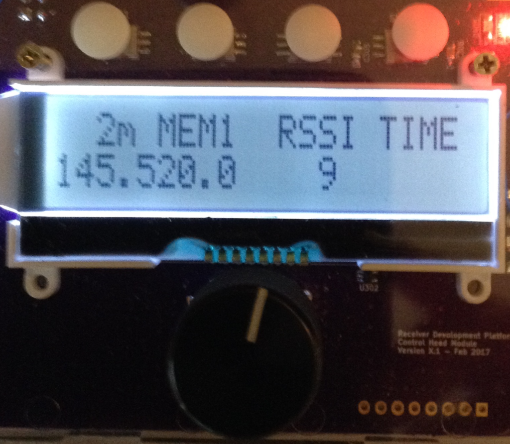
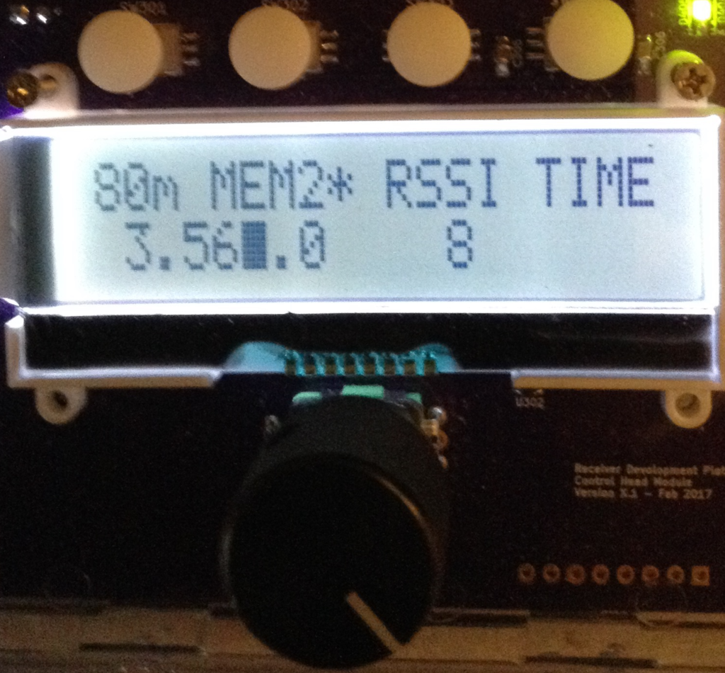
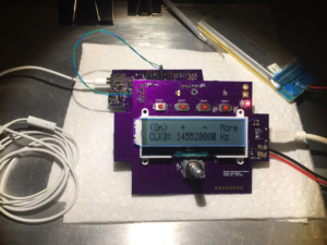
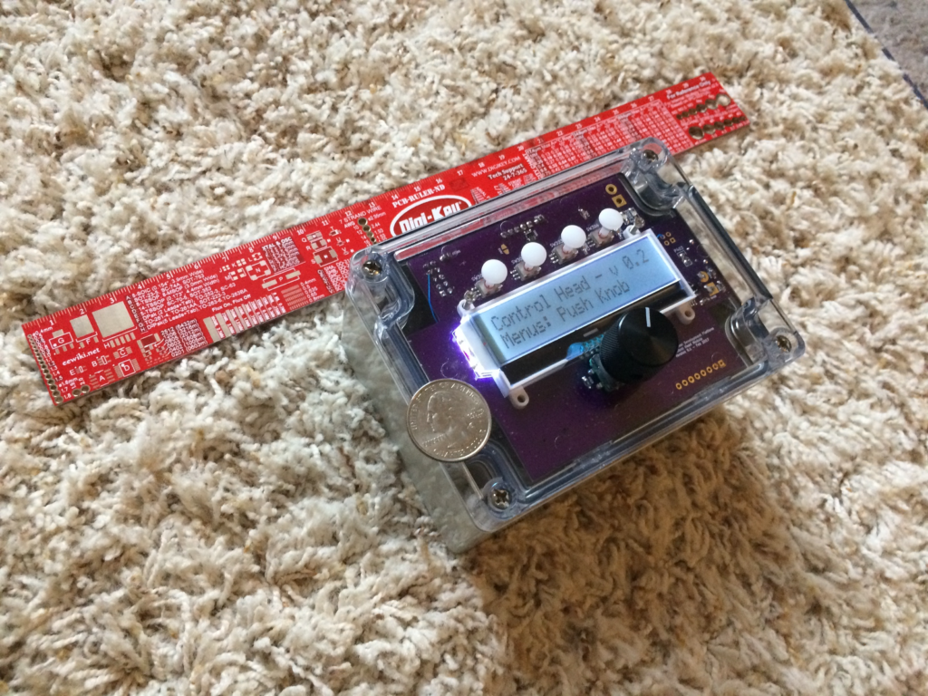
The ruler and quarter provide a sense of scale: the box is easily held in one hand, but it fills the hand. The box is large enough to hold the entire 2-band receiver, and a battery. The four white dots are the button plungers mentioned above, and serve as the “menu” buttons. The black knob below the display operates the rotary encoder, which can be pressed to activate a fifth button.

Firmware now includes a linkbus (inter-processor communication), allowing the Control Head to communicate with and control the Digital Interface, and thus the receiver. The Receiver board has not yet been populated.

The Control Head can now instruct the Digital Interface to fully configure the Si5351 clock chip, set the main volume, the tone volume, and report ADC readings. We are getting close to having a platform that can support receiver debugging and testing.


Control Head and Digital Interface Rev X1

This post concerns the Open ARDF Equipment Project, which is utilizing the Receiver Development Platform, both of which are being developed together.

The first Rev X1 Control Head and Digital Interface boards are now working together. The Control Head is able to set the frequency of the Si5351 IC on the Digital Interface as shown on the display. Not all of the components have been tested on the Digital Interface yet, and the separate processors are not yet communicating with one another. But at least they are not interfering with one another!

The earphone plugged into the Digital Interface enables the power on both boards. The red LED indicates that the LiPo battery (upper right) is being charged by the USB cable (center right). The twisted pair of wire-wrap wires running between the boards (upper left) is connecting the I2C bus between the two boards.